Click on OK
so that the inputs take into effect. Follow the usual steps to specify
the type
of Analysis
to be done and select the outputs to be plotted.
4) This step is
very important. If you have any doubts please clarify it
in the labs. Once you have completed the
simulation,
make sure you save the state. This can be done by selecting "Setup -> Save state" menu
from the SimW (Affirma Analog Design Environment) window. In the Save
state form which pops up
do not change any of the default options. Click Ok to complete save
state.
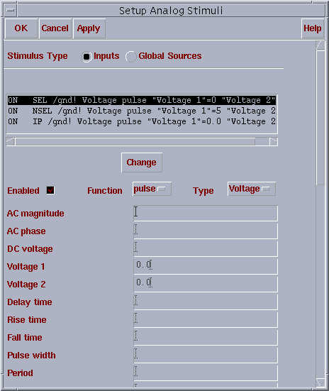
5) Specify the inputs
for all the schematic created using the above method. Once the simulation
is complete
save the state for all the cells.
Library Structure Required:
You will be submitting the cadence library
where you created your designs. Name the library
where you will be working as HW1.
Inside this library, create the following cells:
i) Nand - This should contain
the layout of the NAND gate.
ii) Tgate - This should contain the layout
of the transmission gate.
iii) Adder - contains the schematic
of the Four bit adder.
Apart from these cells, there can
be other cells in your library which are used as part
of your design. We
will be looking only at the above mentioned cells for grading.
Also, submit a simulated spectre output waveform
snapshots, naming them as Nand_sim, Tgate_sim and Adder_sim respectively.
You will tar and gzip the unix directory corresponding to the cadence library and submit it.
tar cvf HW1.tar
HW1
gzip HW1.tar
submit_cse497 HW1.tar.gz
submit_cse597 HW1.tar.gz
Submit commands can be run from your eng machines.
(You might use Zip utility instead
of tar, if you prefer; zip -r HW1 HW1)