CSE 493/593 Fall 2021
Lab Assignments
Project shared
space information
Project groups
Pad frame
information
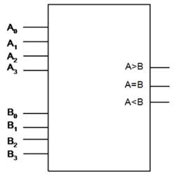
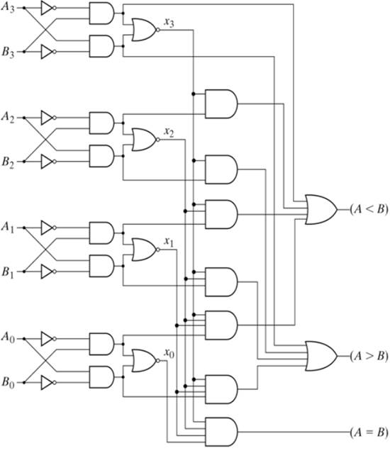
Lab 4: Implementation of a 4-bit Unsigned Magnitude Comparator using Complementary CMOS Logic Gates (10/07/2021 & 10/11/2021):
During simulation, use the following model files:
/util/cadence/local/ncsu-cdk-1.6.0.beta-20150506/models/spectre/standalone/ami06N.m
and
/util/cadence/local/ncsu-cdk-1.6.0.beta-20150506/models/spectre/standalone/ami06P.m
For this lab, you will have to
implement a 4-bit Unsigned Magnitude Comparator with two 4-bit inputs and three
1-bit outputs.
Create symbols
for the schematic, design the layout, extract the layout, simulate the
extracted view and run LVS match checker between the schematic and extracted
views.
Useful Tips:
i. Apply stimuli in such a way that
during a single transient analysis, the output can be verified for at least 10
combinations of inputs.
ii. Keep the width of the PMOS transistors triple the
width of the NMOS transistors. The width of the NMOS and PMOS transistors should be
1.5um and 4.5um, respectively. Their lengths can both be set to 0.6um.
iii. If your design requires, you can reuse the gates
designed in Lab 1
Lab 3: Implementation of a 4-bit
Complementary CMOS Ripple Carry Adder
(9/30/2021 & 10/04/2021):
During simulation, use the following model files:
/util/cadence/local/ncsu-cdk-1.6.0.beta-20150506/models/spectre/standalone/ami06N.m
and
/util/cadence/local/ncsu-cdk-1.6.0.beta-20150506/models/spectre/standalone/ami06P.m
For this lab, you will have to
implement a Static CMOS 4-bit RCA using four 1-bit full adders.
First, design a 1-bit full adder
circuit (Schematic and Layout level) and simulate to verify if our design
follows the truth table. You can create a symbol and use this to construct a
4-bit Ripple Carry Adder.
Create symbols
for each schematic, design the layout, extract the layout, simulate the
extracted view and run LVS match checker between the schematic and extracted
views.
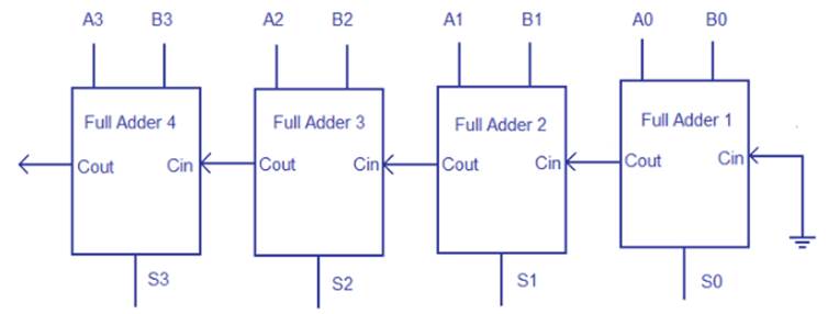
4-bit RCA
Useful tips:
i. Apply stimuli in such a way that
during a single transient analysis, the output can be verified for at least 5
combinations of inputs.
ii. Keep the width of the PMOS transistors triple the
width of the NMOS transistors. The width of the NMOS and PMOS transistors should be
1.5um and 4.5um, respectively. Their lengths can both be set to 0.6um.
iii. If your design requires, you can reuse the gates
designed in Lab 0 and Lab 1.
Lab 2: Implementation of a positive
edge-triggered D Flip Flop (9/23/2021 & 9/27/2021):
During simulation, use the following model files:
/util/cadence/local/ncsu-cdk-1.6.0.beta-20150506/models/spectre/standalone/ami06N.m
and /util/cadence/local/ncsu-cdk-1.6.0.beta-20150506/models/spectre/standalone/ami06P.m
For this lab, you will have to
implement a positive edge-triggered D Flip Flop using
i. Complementary CMOS Logic
ii. Transmission Gate Logic
Create symbols
for each latch schematic, design the layout, extract the layout, simulate the
extracted view and run LVS match checker between the schematic and extracted
views.
Use the
designed latches to create the flip-flops and complete the schematic, layout,
simulations of the schematic and extracted views and LVS match.
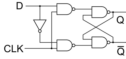
D Latch using NAND gates
Useful tips:
i. It is recommended that you go through the lecture material
that covers designing Complementary CMOS circuits and Transmission gate logic
circuits (Lecture 1 on course website and Chapters 6.2.1, 7.2.4 in the text
book)
ii. Familiarize
yourself with the difference between flipflops and latches.
iii. During simulation, make sure your stimuli (D and
CLK) do not have same rising and falling edges. You should be able to
demonstrate the functioning of the DFF for all cases and combinations of
inputs.
iv. Keep the width of the PMOS transistors triple the
width of the NMOS transistors. The width of the NMOS and PMOS transistors should be
1.5um and 4.5um, respectively. Their lengths can both be set to 0.6um.
Consider rise time and fall time to be 0.01ns.
v. If your design requires, you can reuse the gates
designed in Lab 0 and 1.
Lab 1: Implementation of Basic Logic
Gates: NAND, NOR, XOR (9/16/2021 & 9/20/2021):
During simulation, use the following model files:
/util/cadence/local/ncsu-cdk-1.6.0.beta-20150506/models/spectre/standalone/ami06N.m
and
/util/cadence/local/ncsu-cdk-1.6.0.beta-20150506/models/spectre/standalone/ami06P.m
For this lab,
you will have to implement the basic 2-input gates
i.
NAND
ii.
NOR
iii.
XOR
Create symbols
for each schematic, design the layout, extract the layout, simulate the
extracted view and run LVS match checker between the schematic and extracted
views.
Useful tips:
1. Another important thing to note is to keep the
width of the PMOS transistors triple the width of the NMOS transistors. The width
of the NMOS and PMOS transistors should be 1.5um and 4.5um, respectively. Their
lengths can both be set to 0.6um.
2. As you have to design 2-input gates, you should test
your circuit for all possible combination of inputs. This can be done using two
pulse inputs, one with twice the time period of the other. Another effective
method to give stimuli is using bit inputs with 0.01ns rise and fall times.
Lab 0: Introduction to VLSI Lab -
Cadence Tutorial (09/09/2021 & 09/13/2021):
It
is highly recommended that you go over the Cadence setup and tutorial
pages as you work on this assignment to correctly setup your tool and access.
Follow all steps given under Cadence setup. The documentation provided under
the help menu in each cadence tool also contains detailed information on using
the tools.
Lab assignment:
Design
a CMOS inverter in Cadence. The width of the NMOS and PMOS transistors should
be 1.5um and 3um, respectively. Their lengths can both be set to 0.6um. For
simulations, set the inverter input signal to have a rise time of 0.5ns, fall
time of 0.5ns, pulse width of 2ns, period of 5ns.
- Create the inverter schematic using Virtuoso
Schematic L
- Simulate the inverter using Spectre
simulator in the Analog Design Environment L tool. Measure the propagation
delay of the inverter in the waveform window
- Create an inverter symbol using Virtuoso Schematic L
- Layout the inverter in Virtuoso Layout XL. Extract
the layout and simulate it. Measure the propagation delay of the inverter
in the waveform window
- Is there a difference in the propagation delays
between the circuit schematic and layout? Why/Why not?
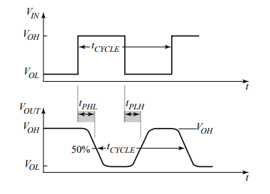
Propagation Delay (tp):
Propagation delay expresses the delay experienced by a signal when passing
through a gate. tpLH defines the response time of the
gate for a low to high output transition, while tpHL
refers to a high to low transition. The overall propagation delay is
conservatively defined as the average of the two delays tpLH
and tpHL.