CSE 493/593 Fall 2022
Pad Frame Information
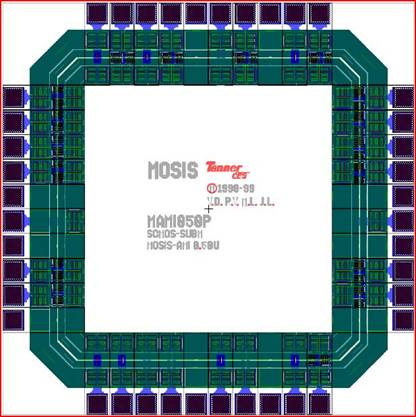
Your final project layout should fit inside
the TinyChip pad frame. It has a total of 40 pins
that can be used to supply Vdd, GND and other input/output
signals to the circuit. The layout view of the pad frame looks similar to this.

The dimensions of the chip along with the pad
frame are 1.5mm x 1.5mm. The inside area of the pad frame that is available to
place your circuit is 900um x 900um.
Please make sure that your circuit can fit in this area. So, it would be easier
to have the dimensions in mind from the very start so that you can plan your
design layout appropriately. You will be placing the layout inside the padframe and not the schematic.
Each pin/pad in the pad frame is one of
following 8 types
|
PADFC |
Pad frame corner, non-usable |
|
PADAREF |
Analog reference pad, non-usable |
|
PADGND |
Pad ground, 1 pad |
|
PADINC |
Buffered input pad: The input signal to chip received at the pad is
buffered and the signal and its complement made available to the circuit
inside, 9 pads |
|
PADIO |
Input/output pad, 7 pads |
|
PADNC |
Spacer pad, non-usable |
|
PADOUT |
Output pad with buffer, 8 pads |
|
PADVDD |
Vdd
power pad, 1 pad |
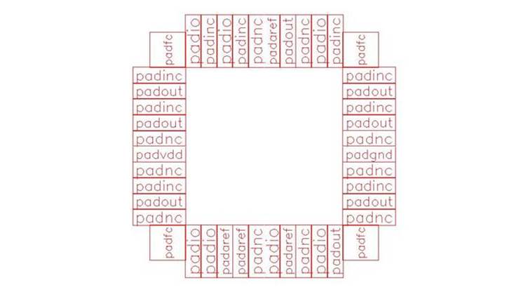
So the total number of pads available to you is
Vdd (1), Gnd (1), Input
(9), Output (8), Input/Output (7). The arrangement of
these pads in the pad frame is shown below -

Detailed information about the pad frame is
available here.
Integrating your final project layout with the pad
frame:
Note:
An example circuit named inverter_padframe
is available for your reference in the AMI_PADS library.
Step 1: In the File Manager window, click on
Edit > Library Path. Include the following library and save.
Library name: AMI_PADS
Library path: /util/cadence/CSE493_593/AMI_PADS
After this step, you should see the AMI_PADS
added to the list of libraries in your library manager.
Step 2: In your final project library, create
a new layout cell view called teamX (where X is your
team ID). In the layout window, instantiate the min_frame
layout_nodrc
cell view from the AMI_PADS library. Next, instantiate your own project layout
and place it inside the pad frame. Save the layout.
Connecting your circuit to the pad frame:
Note: An example circuit named inverter_padframe
is available for your reference in the AMI_PADS library.
Step 1: To connect an input signal labeled
“A1 in your circuit to the pad frame, do the following: Since A1 is an input signal,
it should be connected to a padinc or a padio pad. If it is an output signal, padout or padio will work. Let’s say we do this with a padinc pad in this example. So
identify a padinc
pad that is not yet connected to any other signal/net in the circuit. Create a
pin in metal 3 layer by clicking on first clicking on metal 3 in the LSW window
and then Create>Pin in the layout window. Name this pin A1 and place it
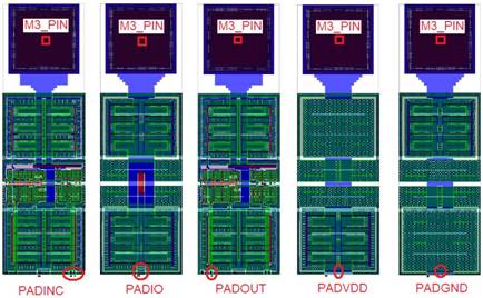
right in the middle of the chosen padinc pad. In the picture below, this corresponds to the
location of the red rectangle marked M3_PIN in the pads.

Step 2: Identify the “A1 point in your
circuit and route a wire from that point to the connection location on the
chosen padinc’s pad. The connection location in the pad
varies depending on the type of pad. In the figure above, the red circle
towards the bottom of the pad shows the connection location for each type of
pad. Except padvdd
and padgnd,
all connection locations are in the metal 2 layer. This means that even if you
have routed your A1 signal on different metal layers to get to the connection
location of the pad, make sure you switch to metal 2 layer to actually connect
to the pad. The padvdd
and padgnd
connection locations are on metal 1 layer. It is a good idea to ensure the vdd and gnd wires are wider than
other wires.
Important: It is a good idea to frequently
perform DRC checks on the layout after routing signals to the pads. This will
ensure that you don’t have to sit down with debugging the entire circuit at one
go later on. When you do perform these DRC errors, ignore the “No geometries
for this pin errors if you get any.
Repeat this process for all signals in your
circuit, and for vdd and gnd. It is a good idea to
use one metal (e.g. metal 1) for all horizontal routing and the other metal
layer (e.g. metal 2) for all vertical routing. That will make the overall
routing easier. But this is no hard and fast rule. You could make changes to it
as you see fit.
Simulating the circuit along with the pad frame:
Note: An example circuit named inverter_padframe
is available for your reference in the AMI_PADS library.
Step 1: So after you connect your circuit to
the pad frame and have routed all signals correctly, a drc
check on your circuit should generate only the “no geometry for this pin
errors. At this point, right click on the min_frame instantiation and select
its properties. Change the layout_nodrc to layout. Then re-run the DRC check. This
time, it should produce exactly 2093 errors. If it produces more than this,
change the min_frame back to layout_nodrc
and then run DRC again to make sure the only errors are “no geometry for this
pin errors.
Step2: With exactly 2093 errors in the DRC,
save your design and extract it with the parasitic caps switch (the first one
in the list) selected. You may now simulate the extracted circuit similar to
your earlier lab assignments. Use the results browser to plot the waveforms.
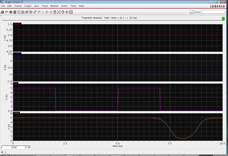
The simulation waveforms from the example
circuit inverter_padframe in the AMI_PADS library is
shown below:
