Study Material, Topics and Sections
April 30 by Bina
- Chapter 4: Section 4.9: Decoders
2X4 decoders, 3X8 decoders, 3X16 decoders
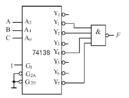
NAND output decoder: figure 4.19; build combinational circuit
- Chapter 4: Section 4.12 Verilog Descrition of Combinational circuit
Verilog (structural) description of gate circuit (like hwk5, lab1), but with a test bench. p.181.
- Chapter 5: Section 5.5 Analysis of sequential circuits
Given a cicuit (see fig.5.15) get the state equations, state table, state diagram.
- Chapter 5: Section 5.6 Verilog Description of Sequential Circuit
Behavioral verilog model. Example 5.7 of p.215,229
- Chapter 5: Section 5.8: Synthesis of sequential circuits
Synthesis with JK, T and D FF. Problem statement, state diagram, state table, FF input equations, FF diagram.
- Chapter 6: Section 6.5: Counter with unused state
Upto p.282.
- Chapter 7: Section 7.6: Programmable Logic Array
- Data Representation: Classnotes, online information. IEEE 754 standard for floating point reprsentation. Given a number in real number format (75.42) represent in IEEE 752 format.
Extra Problems
Exercises: 5.10, 5.20, 5.49, 6.24, 6.27, 7.28
Sample Questions
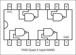
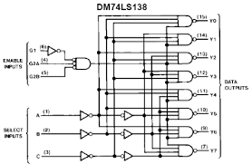
- Design a combinational circuit using a 3X8 decoder such as 74LS138 and NAND gates chip such as 74LS00: F1(X,Y,Z) = ∑(m3,m5,m7).
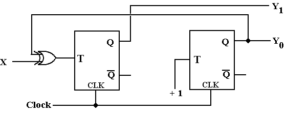
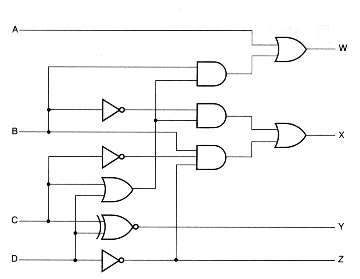
- Analyze the sequential circuit given below.
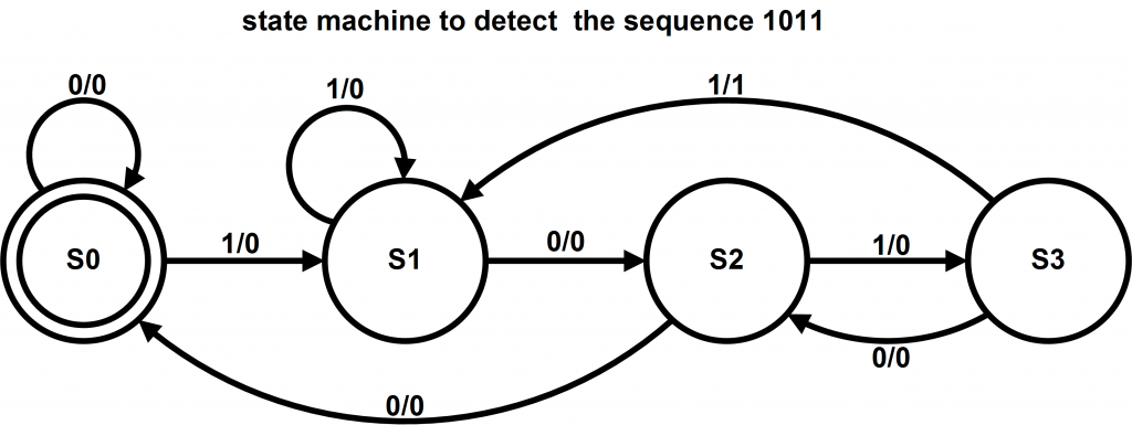
- Synthesize a sequential circuit defined by the finate state machien given below:
- Design the counter that counts the sequence (0,2,3,4,6). Use D-FF.
- Write the Verilog description of the combinational circuit given below and provide the testbench to simulate and test your descrption.
Like Hwk1.
- Write the Verilog Description of the sequential circuit given below and provide the test bench.
-
Implement the functions F1 and F2 gievn below using a PLA (NOT,AND,OR,XOR stages).
F1(A,B,C) = AB+C'B'+CA'
F2(A,B,C) = (AB+B'A'+C'A')'
- Labs 1-4 material.
- IEEE 754 floating point representation.