Digital Systems
CSE241 Digital Systems
Classnotes
Classnotes
| Date | Topic | Chapter | Classnotes |
|---|---|---|---|
| 1/30 | Course Goals and Plans | Course description | C1 |
| 2/1 | Number System | Chapter 1 | C2 |
| 2/3 | Signed Arithmetic | Chapter 1 | C3 |
| 2/6 | Boolean Algebra | Chapter 2 | C4 |
| 2/8,2/10 | Boolean Algebraic Simplification | Chapter 2 | C5 |
| 2/13 | Logic gates and IC chips | Chapter 2 | C5 |
| 2/15 | Karnuagh Map | Chapter 2 | C6 |
| 2/17 | Lab 1 Complete demo | Lab 1 | C7 |
| 2/20 | K-map simplification | Chapter 3 | C8 |
| 2/22 | Problem Solving using Logic Gates | Chapter 3 | C8 |
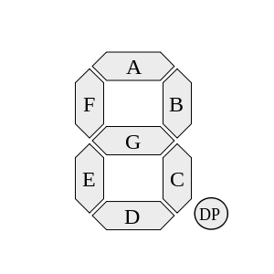
| 2/24 | Seven segment LED Display | Chapter 3 | C9 |
| 2/27 | Analysis of Combinational Circuits | Chapter 4 | C10 |
| 3/1 | MSI: Full Adder | Chapter 4 | C11 |
| 3/3 | MSI: Decoder | Chapter 4 | C12 |
| 3/3 | MSI: Multiplxer | Chapter 4 | C13 |
| 3/8,10 | Midterm Exam Review | Chapter 1-4 | |
| 3/13 | Midterm Exam | Chapter 1-4 | |
| 3/17 | Floating Point Representation | Classnotes | C14 |
| 3/29 | Introduction to Sequential Circuit | Chapter 5 | C15 |
| 3/31 | Sequential Circuit Analysis | Chapter 5 | C16 |
| 4/3 | Sequential Circuit Synthesis | Chapter 5 | C17 |
| 4/5 | Data-intensive Computing Certificate Program | Review Analysis of SeqCkt | C18 |
| 4/10,12 | Hardwre Description Language | Chapter 3 | C17 |
| 4/17 | Verilog: Sequential Circuit Description | Chapter 5 | C18 |
| 4/19,21 | Field programmable Logic Array | Chapter 7 | C19 |
| 4/24 | FPGA Programming | Lab 4 | |
| 5/1 | Final Exam Review | C20 | |
| 5/3 | Floating point | C21 | |
| 5/6 | What's my grade standing in class? | My Grade so far |
Number Systems
Consider playing cards, set of coins: how do understand these systems?
We think in decimal, computers number crunch in binary
How do you define a number system?
Radix of a number system?
Number conversion
Decimal to binary, binary to decimal
Numbers with fractions
ASCII 7-bit code for information representation
Notes
Signed Integer Arithmetic
ASCII 7-bit code for representation of characters.. standard code
BCD for binary form of decimal
Representing numbers for efficient computation: 1's complement and 2's complement
In general, lot of research effort on "coding" information for efficient and reliable processing: excess-3 code, Gray code
Binary arithmetic: sign-magnitude vs. 2's complement
Signed Binary Arithmetic Consider numbers A = 53 and B= 76. Assume positive numbers are represented using sign-magnitude and negative numbers as 2's complement. Perform the operations below in binary. Assume 8-bit container. Specify if the result is positive, negative or overflow and explain your answer.
- X = A + B
- Y = A - B
- Z = -A -B
- W = -A + B
Notes
Boolean Algebra
Boolean algebra is like any other math system: Set of elements, set of operators, and a number of axioms and postulates.
Basic operations {AND, OR, NOT} {.,+,'}
Most common postulates:
1. Closure: w.r.t an operator is closed if for every pair of elements of S, the binary operator results in a unique value in the S.
2. Associative: (x*y)*z = x*(y*z)
3. Commutative: x * y = y *x
4. Identity element: e *x = x*e = x where e is the identity element
5. Inverse element: x *x' = 0
We can repeat all these w.r.t to + operator.
Theorems:
x+x = x x*x =x
(x')' = x involution
x + (y + z) = (x+y)+z associative
x*(y + z) = x*y + x*z distributive
De Morgan's law: (x + y)' = x' * y'
x + xy = x Absorption law x (x+y) = x
Operator precedence: (i) parentheses (ii) NOT (iii) AND (iv) OR
Implementation of Boolean functions:
f1 = x + y'z
F2 = x'y'z + x'yz + xy' ---> F2= xy' + x'z
Algebraic simplification: goal is to minimize the Boolean function to minimum number of literals and minimum number of terms. We will use only sum of products form.
F1 = x + xy
F2 = xy + x'z + yz
Minterm --- product term -? canonical form : sum of minterms
Maxterm --- sum term -? canonical form: product of maxterms
Standard forms of Boolean expressions.
Notes
Boolean Algebraic Simplification
Lets review what we did last class.
What is simplification of a Boolean expression? Goal of simplification is to minimize the number of literals and also the number of terms in an
expression. We will look at algebraic simplification by applying the laws and theorems.
We will implement the Boolean expressions uisng logic gates. {AND, OR, NOT} combiation and also using only NAND gate. We will also implelemt the circuits using common IC chips.
Logic gates are used to implement Boolean functions. For the gates, study it through the name of the gate, logic operator, graphic symbol, truth table and expression representing the operation of a gate.
Boolean Functions
We will discuss implementation of Boolean functions. Here are the steps in the design and implementation of a Boolean function.
- Problem statement
- Truth table
- Sum of minterms expresions
- Simplification or minimization of the expression
- Implementation using logic gates
Problem Statement: Design a combinational logic circuit to generate odd parity for the BCD code; a logic circuit that will generate the odd parity bit for any 4-bit combination of the BCD code. Implement it using (i) {AND, OR, NOT} and (iii) using only NAND gates.
What is BCD code? Binary Coded Decimal. It is a 4-bit binaty code representing the decimal digits {0..9}.
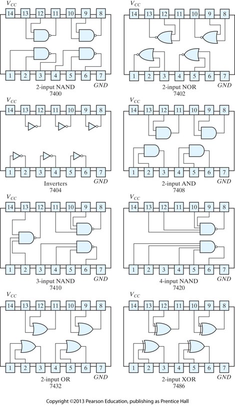
Logic Gates and IC Chips
Lets review what we did last class: we worked on solving a simple problem. We are yet to complete an efficient gate design for the problem. We need some more information about logic gates. Lets do that today.
We are in Chapter 2.
Logic Gates
Lets go thru all the logic gates. This is given in figure 2.5: AND, OR, NOT, Buffer, NAND, NOR, XOR, XNOR.Problem 1
Lets simplify: F(A,B,C) = m1+m4+m5+m6+m7. Implement it using (i) AND , OR, NOT (ii) only NAND gates.Digital ICs
Lets implement the simplified function commonly available logic gates chips.Karnaugh Map
We will explore K-maps for 2-3-4-variable functions.
Lab 1 Demo
We will demo how to work on Lab1.
K-Map Simplification
We will fully explore K-map simplification. We will also revisit out BCD to odd parity generator.
Problem Statement-> Gate Implementation
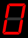
1. We will revisit: BCD to odd parity generator. 2. We will also solve the Decimal to 7-segment LED Display circuit
Problem Statement-> Gate Implementation
We will also solve the Decimal to 7-segment LED Display circuit.
(From Wikipedia)
Analysis of Combinational Circuit
So far we synthesized or designed and constructed circuits. Today we will learn how deconstruct and analyze a combinational circuit. See figure 4.2, p.128. We also designed a half-adder.
MSI Adder Circuit
We designed a full-adder. Sum(A,B,Cin) and Cout(A,B,Cin). Also on use of DeMorgan's law.
MSI Decoder Circuit
We will study MSI circuits for an nX2^n decoder and 2^nX1 MUX. For each of these circuits we will study:
- The block diagram
- Size of the MSI chip, inputs, outputs, control lines
- Building larger circuits with n smaller decoder(/MUX) chips.
- Implementing a combinational circuit using decoder(/MUX) chips.
Introduction to Sequential Circuit
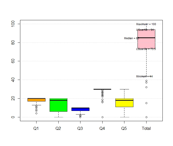
Midterm grade distribution.
We will study sequential circuits using
- Basic components: Flip-flops (FF)
- Major elements: memory (FFs) and circuits driving the FFs
- Analysis of sequential circuit
- Synthesis of sequential circuits
- From problem statement to sequential circuit design
- State diagrams: Finite state machines (FSM) design tool
Verilog Hardware Desription Language: Chapter 3
Boolean algebraic simplification is good for explaining the fundamentals; K-map is good for
further formalizing the simplification process. However for function with more than 4 variables, these methods DO NOT scale well.
We need better ways of decribing the hardware so that the process of implementing (manufacturing) and testing can be scaled up
and automated for LSI, VLSI and onwards. Hardware Description Languages (HDL) such as Verilog are solutions that address the scalability and automation issues.
We will look at only Verilog.
Here is an introductory Presentation on Verilog
Getting Started with Verilog
This page provides some useful information about gettign started with verilog.
- How to access CSE server using Putty
- How to compile verilog code?
- Notes from a Ex-UTA for this course: JD's notes
4-bit Adder Verilog description with test bench
Adder.vVerilog Description of Sequential Circuit
Here is a complete example of a simple 2-bit counter shown in the figure on the right. In this diagram, x is the input for counting and y is the output.The verilog code for the circuit and the test bench is shown below:
// Sequential Circuit Example 5_20 : the instantiation is inside
// the test bench
// item 1
module counter2 (output y, input x, input clock,input reset);
// item 2
   reg[1:0] state;  // 2 bits
// item 3
   parameter S0=2'b00, S1 = 2'b01, S2=2'b10, S3=2'b11;
//item 4 when and how do the state transitions happen?
   always@ (posedge clock, negedge reset)// event driven
     if (reset == 0) state <= S0;
     else case (state)
	    S0 : if(x==1) state <= S1; else state<= S0;
            S1 : if(x==1) state <= S2; else state<= S1;
            S2 : if(x == 1) state <= S3; else state<= S2;
            S3 : if(x == 1) state <= S0; else state<= S3;
	  endcase // case(state)
// item 5 : output
   assign    y = (state==S3);
endmodule // counter2

module counter2_tb;
   // stand alone
 // item 1 definitions
   reg x, clk, rst;
   wire y;

 // item 2 instantiate counter2
   counter2 C1(y, x, clk,rst);
 // item 3
   initial #200 $finish; // duration of your simulation testing
// item 4
   initial begin
      rst = 0;
      clk = 0;
      #5 rst = 1;

      repeat (16)
	#5  clk = ~clk;
   end

// item 5 for x
initial begin
 x = 1'b0;
 repeat(8)
 #10 x = ~x;
end
// item 6 for montioring, output text and waveform
initial begin
$monitor("x=   %d  y= %d",x,y);
$dumpfile("example1.vcd");
$dumpvars;
end
endmodule
Commands for compiling and simulating the Verilog code.
iverilog -o example1.vvp example1.v
vvp example1.vvp
gtkwave example1.vcd
Memeory and Programmable Logic: Chapter 7
How do we scale up and automate the process of synthesis of circuits that we learned so far.
Consider a combinational circits and its block diagram as shown below.
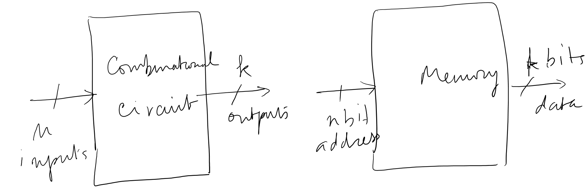
Combinational circuit has n inputs, k outputs. The memory on the right has n bits address and k bits data. Here lies a great idea, a "disruptive" one: Why dont we replace the block of gates with block of memory lcoation and program them with appropriate data. Porgrammable Read Only Memory (PROM) model of programmable logic.
Here is another idea: if we have n variables, the number of minterms is 2^n. These can be formed using 2^n AND gates. If there are k outputs, there are k functions. We can implment the k functions using the minterms we formed earlier and k OR gates. Here is an idea: if we can pre-create the minterms, and allow the OR gates to be programmed,then we have programmable gate array (PGA) and if we can program it "in field" we have field programmable gate array or FPGA
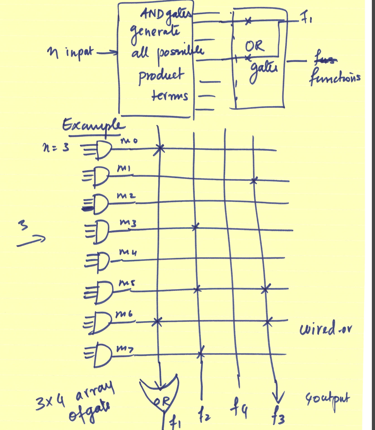 Lets work on a problem to understand the "FPGA" concept.
Example 7.2 from your text book. Implement these function using an FPGA.
F1(A,B,C) = ∑(0,1,2,4)
F2(A,B,C) = ∑(0,5,6,7
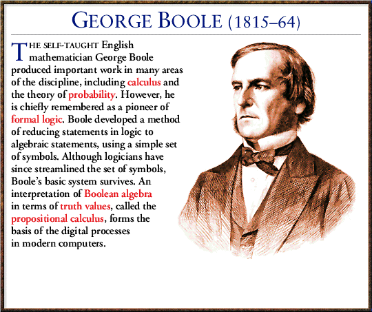
George Boole
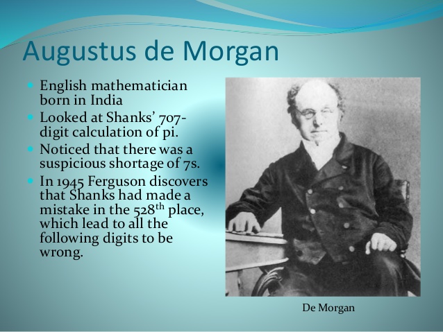
Augustus Demorgan
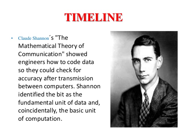
Claude Shannon
Katherine Johnson

Logic Gate ICs
Maurice Karnaugh
Decimal Keyboard
Kepler 452b
Nathaniel's Nutmeg

Icarus Verilog

Icarus

10000 hours from Novice to an Expert

2001 Space Odyssey