Lab Notes
Lab4: Verilog Design And FPGA Implementation
Lab 4: Verilog Programming with Xilinx FPGA Board

Pre-lab: We will simulate a decoder combinational circuit on the FPGAboard. We will first define the
bahavior of a decoder using Verilog, syhthesize and implement its design, generate bitstream and experiment with its operation using Xylinx FPGA boards.

What to do?
1. Install Vivado webpack  environment on your laptop. If you dont have a laptop or if you
cannot install it, go to one of TA's office hours:

2. We will work on a demo of a decoder design during lectures this week.

3. I will provide you the steps in the workflow:
Verilog source-->Synthesis-->Implementation-->Bitstream Generation-->ProgramFPGA
We demonstrated this for a 3X8 decoder during this week's recitation.

4. The example I worked out in class can be found here. Stop at p.9:
http://users.wpi.edu/~rjduck/Basys3%20Vivado%20Decoder%20Tutorial.pdf

5. TAs each have an FPGA board. Once you have your bitstream ready,
you dont have to wait till next recitation. Go to TA office hours and
get it verified.

7. You will complete this problem and demo it to your TA during recitation next
week(5/1/2017) or during any of the office hours to get your grade. Thats it.
No submission. Just a demo to your TA the process and outcomes.
Code used in the lab demo: decoder.v and decoder.xdc.
Decoder circuit
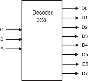
A Decoder & Verilog Code